Integrated Circuits

The CD4070B contains four independent Exclusive-OR gates. The CD4070B provides the system designer with a means for direct implementation of the Exclusive-OR functions, respectively. Features:
- High-Voltage Types (20V Rating)
- CD4070B - Quad Exclusive-OR Gate
- Medium Speed Operation
- tPHL, tPLH = 65ns (Typ) at VDD = 10V, CL = 50pF
- 100% Tested for Quiescent Current at 20V
- Standardized Symmetrical Output Characteristics
- 5V, 10V and 15V Parametric Ratings
- Maximum Input Current of 1µA at 18V Over Full Package Temperature Range
- 100nA at 18V and 25°C
- Noise Margin (Over Full Package Temperature Range)
- 1V at VDD = 5V, 2V at VDD = 10V, 2.5V at VDD = 15V
- Meets All Requirements of JEDEC Standard No.
Please Log In to view prices

The SSI2130 offers unprecedented performance and features, but its ultra-compact QFN package can present prototyping challenges. The EVB2130 eases evaluation by providing a PCB that allows comprehensive exploration of capabilities. The EVB2130-P is fully populated and ready for the bench. With the exception of the SSI2130, all components are through-hole for easy construction and experimentation. A on-board +5V regulator and 2.5V reference simplify external power connections, and pots are provided for mixer control, PWM, and VCO setup. Switches ease selection of saw ramp direction plus Through-Zero and Pulse Modulation. Features
- PCB size: 108 x 82mm
- External Power: ±12V
- Inputs: Expo Freq 1V/Oct PWM In Aux 1 and 2 In FM In PM In Hard Sync Soft Sync
- Outputs: Sine Saw Triangle Pulse Square Mix Out
Please Log In to view prices

The CD4050B devices are noninverting hex buffers, and feature logic-level conversion using only one supply voltage (VCC). The input-signal high level (VIH) can exceed the VCC supply voltage when these devices are used for logic level conversions. These devices are intended for use as CMOS to DTL or TTL converters and can drive directly two DTL or TTL loads. (VCC = 5 V, VOL ≤ 0.4 V, and IOL ≥ 3.3 mA.) Features:
Applications
- Noninverting
- High Sink Current for Driving 2 TTL Loads
- High-to-Low Level Logic Conversion
- 100% Tested for Quiescent Current at 20 V
- Maximum Input Current of 1 µA at 18 V Over Full
- Package Temperature Range; 100 nA at 18 V and 25°C
- 5-V, 10-V, and 15-V Parametric Ratings
Applications
- CMOS to DTL or TTL Hex Converters
- CMOS Current Sink or Source Drivers
- CMOS High-to-Low Logic Level Converters
Please Log In to view prices

CD4071B OR gates provide the system designer with direct implementation of the positive-logic OR function and supplement the existing family of CMOS gates. Features:
- Medium-Speed Operation - tPLH, tPHL = 60 ns (typ.) at VDD = 10 V
- 100% tested for quiescent current at 20 V
- Maximum input current of 1 µA at 18 V over full package-temperature range; 100 nA at 18 V and 25°C
- Standardized, symmetrical output characteristics
- Noise margin (full package-temperature range):
- 1 V at VDD = 5 V
- 2 V at VDD = 10 V
- 2.5 V at VDD = 15 V
- 5-V, 10-V, and 15-V parametric ratings
- Meets all requirements of JEDEC Tentative Standard No. 13B, "Standard Specifications for Description of ’B’ Series CMOS Devices"
Please Log In to view prices

The CD4077B contains four independent Exclusive-NOR gates. The CD4077B provides the system designer with a means for direct implementation of the Exclusive-NOR functions, respectively. Features:
- High-Voltage Types (20V Rating)
- CD4077B - Quad Exclusive-NOR Gate
- Medium Speed Operation
- tPHL, tPLH = 65ns (Typ) at VDD = 10V, CL = 50pF
- 100% Tested for Quiescent Current at 20V
- Standardized Symmetrical Output Characteristics
- 5V, 10V and 15V Parametric Ratings
- Maximum Input Current of 1µA at 18V Over Full Package Temperature Range
- 100nA at 18V and 25°C
- Noise Margin (Over Full Package Temperature Range)
- 1V at VDD = 5V, 2V at VDD = 10V, 2.5V at VDD = 15V
- Meets All Requirements of JEDEC Standard No.
Please Log In to view prices

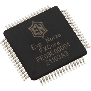
FXCore from Experimental Noize is a DSP designed for creating audio effects in pro-audio devices. FXCore can operate as a standalone device when paired with appropriate CODECs where it generates all necessary clocks or as part of a more complex system where it will lock to the word clock and bit clock provided by another part of the system.
FXCore can store up to 16 programs and their associated register preset values in its internal FLASH memory so no external program storage is required.
FXCore can store up to 16 programs and their associated register preset values in its internal FLASH memory so no external program storage is required.
Please Log In to view prices

