Integrated Circuits
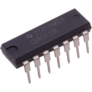
CMOS - CD4011, 2-Input CMOS NAND Gates, 14-Pin DIP
CD4011B NAND gates provide the system designer with direct implementation of the NAND function and supplement the existing family of CMOS gates. All inputs and outputs are buffered. Features:
- Propagation delay time = 60 ns (typ.) at CL = 50 pF, VDD = 10 V
- Buffered inputs and outputs
- Standardized symmetrical output characteristics
- Maximum input current of 1 µA at 18 V over-full package temperature range; 100 nA at 18 V and 25°C
- 100% tested for quiescent current at 20 V
- 5-V, 10-V, and 15-V parametric ratings
- Noise margin (over full package temperature range:
- 1 V at VDD = 5 V
- 2 V at VDD = 10 V
- 2.5 at VDD = 15 V
- Meets all requirements of JEDEC Tentative Standard No. 13B, "Standard Specifications for Description of "B" Series CMOS Devices"
Please Log In to view prices
OTA - AS3280, Dual, Linearizing Diodes, Alfa, 16-Pin DIP
The AS3280 is Alfa’s version of the CA3280 IC. The AS3280 consists of two variable operational amplifiers that are designed to substantially reduce the initial input offset voltage and the offset voltage variation with respect to changes in programming current. This design results in reduced "AGC thump," an objectionable characteristic of many AGC systems. Careful design of critical places of the circuit reduces the amplifier dependence upon thermal and processing variables.
The AS3280 has all the generic characteristics of an operational voltage amplifier except that the forward transfer characteristics is best described by transconductance rather than voltage gain, and the output is current, not voltage. The magnitude of the output current is equal to the product of transconductance and the input voltage.
The AS3280 has all the generic characteristics of an operational voltage amplifier except that the forward transfer characteristics is best described by transconductance rather than voltage gain, and the output is current, not voltage. The magnitude of the output current is equal to the product of transconductance and the input voltage.
Please Log In to view prices
CMOS - CD4007, Dual Complementary Pair Plus Inverter, 14-Pin DIP
CD4007UB types are comprised of three n-channel and three p-channel enhancement-type MOS transistors. The transistor elements are accessible through the package terminals to provide a convenient means for constructing the various typical circuits as shown in Fig. 2. More complex functions are possible using multiple packages. Numbers shown in parentheses indicate terminals that are connected together to form the various configurations listed. Features:
- Standardized symmetrical output characteristics
- Medium Speed Operation — tPHL, tPLH = 30 ns (typ.) at 10 V
- 100% tested for quiescent current at 20 V
- Meets all requirements of JEDEC Tentative Standard No.
Please Log In to view prices
CMOS - CD4015, Dual 4-Stage Static Shift Register, 16-Pin DIP
CD4015B consists of two identical, independent, 4-stage serial-input/parallel-output registers. Each register has independent CLOCK and RESET inputs as well as a single serial DATA input. "Q" outputs are available from each of the four stages on both registers. All register stages are D-type, master-slave flip-flops. The logic level present at the DATA input is transferred into the first register stage and shifted over one stage at each positive-going clock transition. Resetting of all stages is accomplished by a high level on the reset line.
Please Log In to view prices


